Introduction
Multi Layer Printed Circuit Board Assembly (ML PCBs) have emerged as a cornerstone solution, enabling the integration of complex circuitry into a smaller footprint. This article delves into the intricacies of multilayer PCB assembly, exploring its applications, benefits, challenges, and best practices.
In today’s technologically advanced world, the demand for compact, high-performance electronic devices has skyrocketed.
FAQs
Q: What is the difference between a multilayer PCB and a flexible PCB?
A: A multilayer PCB has multiple layers of circuitry stacked on top of each other, while a flexible PCB is made from a flexible substrate that allows for bending and folding.
Q: How many layers can a multilayer printed circuit board assembly have?
A: The number of layers in a multilayer PCB can vary widely, ranging from a few to several dozen.
Q: What are the common materials used for multilayer printed circuit board assembly?
A: Common materials include FR-4 (epoxy glass), high-temperature FR-4, polyimide, and Teflon.
Q: What are the key factors to consider when selecting a multilayer PCB manufacturer?
A: Key factors include manufacturing capabilities, quality control measures, lead times, and pricing.
Q: What are the future trends in multilayer printed circuit board assembly technology?
A: Future trends include the development of even denser PCBs, the use of advanced materials, and the integration of embedded components.
Design and Manufacturing
Q: What are the common design software tools used for multilayer printed circuit board assembly?
A: Popular tools include Altium Designer, Autodesk Eagle, and KiCad.
Q: How do I ensure signal integrity in multilayer printed circuit board assembly?
A: Use impedance-controlled routing, minimize vias, and carefully consider trace lengths and widths.
Q: What factors influence the cost of multilayer printed circuit board assembly?
A: Factors include the number of layers, component density, board size, and manufacturing complexity.
Q: How can I reduce the risk of manufacturing defects in multilayer printed circuit board assembly?
A: Implement robust quality control measures, use high-quality materials, and adhere to industry standards.
Applications and Trends
Q: What are the emerging applications of multilayer printed circuit board assembly in the automotive industry?
A: Advanced driver assistance systems (ADAS), electric vehicles (EVs), and autonomous vehicles are driving the demand for complex multilayer PCBs.
Q: How are multilayer printed circuit board assembly used in wearable technology?
A: Wearable devices often incorporate multilayer PCBs to integrate sensors, processors, and wireless communication modules into a compact form factor.
Q: What are the future trends in multilayer PCB technology?A: Trends include the development of flexible PCBs, embedded components, and advanced materials with improved thermal and electrical properties.
Printed Circuit Board Assembly: A Critical Component in Modern Electronics
Printed circuit board assembly (PCBA) is a crucial process in the manufacturing of electronic devices. It involves the attachment of various electronic components, such as resistors, capacitors, and integrated circuits, onto a printed circuit board (PCB). The PCB serves as a foundation for interconnecting these components, creating functional electrical circuits.
The PCBA process typically involves several key steps:
- Component Preparation: Electronic components are prepared for assembly, often including sorting, inspection, and programming as needed.
- PCB Preparation: The PCB is cleaned and inspected to ensure it is free from contaminants that could affect the assembly process.
- Solder Paste Application: A stencil is used to apply solder paste to the PCB pads, creating a reservoir for the components to be attached.
- Component Placement: Automated machines, known as pick-and-place machines, precisely position the components onto the PCB according to the design data.
- Reflow Soldering: The PCB is heated in a reflow oven to melt the solder paste and create strong connections between the components and the PCB.
- Inspection and Testing: The assembled PCB undergoes rigorous inspection and testing to ensure its functionality and quality.
PCBA is a critical process in a wide range of industries, including electronics, automotive, medical, and audio. It enables the creation of complex electronic devices with miniaturized designs and enhanced performance.
Advancements in PCBA technology, such as automated assembly lines and advanced inspection techniques, have contributed to the increased efficiency and reliability of the process.
Environmental and Sustainability
Q: How can I make my multilayer printed circuit board assembly more environmentally friendly?
A: Choose materials with lower environmental impact, reduce waste during manufacturing, and implement energy-efficient processes.
Q: What are the challenges associated with recycling multilayer printed circuit board assembly?
A: The presence of hazardous materials and the complexity of the manufacturing process can make recycling difficult.
Q: How can I ensure responsible sourcing of materials for my multilayer printed circuit board assembly?
A: Work with suppliers who adhere to ethical and sustainable practices.
Understanding Multilayer Printed Circuit Board Assembly
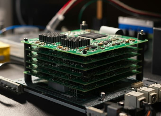
Multi Layer Printed Circuit Board Assembly, as the name suggests, are boards with multiple layers of copper circuitry separated by insulating materials. The layers are interconnected through vias, enabling intricate circuitry and precise component placement. Multilayer PCBs offer distinct advantages over single-layer or double-layer PCBs.
Increased component density: The ability to route traces on multiple layers allows for a higher component count within a given area.
Improved signal integrity: Shorter trace lengths and reduced crosstalk contribute to better signal quality and performance.
Enhanced design flexibility: Multilayer Printed Circuit Board Assembly provides greater design freedom, enabling the creation of complex and innovative circuit layouts.
Applications of Multilayer Printed Circuit Board Assembly
MultilayerPrinted Circuit Board Assembly are widely used across various industries due to their versatility and performance benefits. Some common applications include:
Audio: High-end audio equipment, such as amplifiers, preamps, and digital audio processors, often employ multilayer PCBs to accommodate complex analog and digital circuitry.
Video: Modern televisions, projectors, and video game consoles rely on multilayer printed circuit board assembly to handle high-speed video signals and advanced image processing.
Medical: Medical devices, including diagnostic equipment, surgical instruments, and patient monitoring systems, benefit from the reliability and miniaturization enabled by multilayer multilayer printed circuit board assembly..
Automotive: Advanced driver assistance systems (ADAS), infotainment systems, and electric vehicle (EV) control units often incorporate multilayer printed circuit board assembly to meet the stringent requirements of automotive electronics.
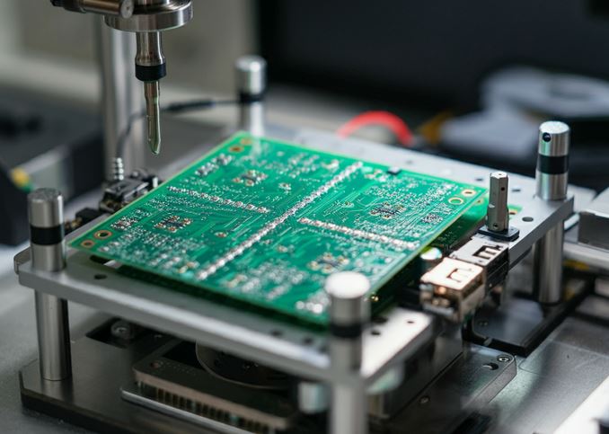
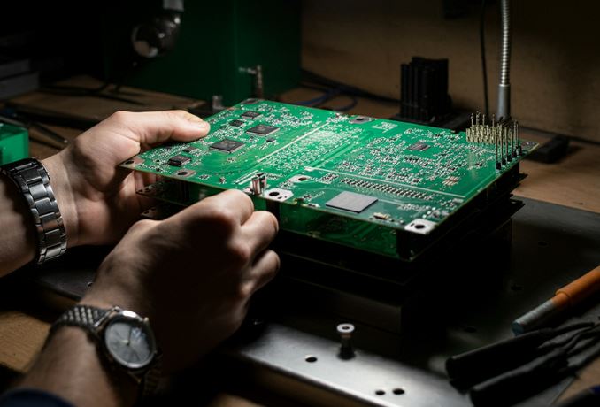
The Multilayer Printed Circuit Board Assembly Process
Multilayer printed circuit board assembly involves several critical steps:
PCB Preparation: The raw PCB is cleaned and inspected to ensure it is free from defects.
Automated pick-and-place machines accurately position components on the PCB, following the design specifications.
Solder Paste Application: A stencil is used to apply solder paste to the PCB pads, creating a solder reservoir for component attachment.Reflow Soldering: The PCB is heated in a reflow oven to melt the solder paste and create strong connections between the components and the PCB.
Inspection and Testing: Automated optical inspection (AOI) and functional testing are performed to verify the quality of the assembly and identify any defects.
Challenges and Considerations
While multilayer printed circuit board assembly offer numerous advantages, their assembly presents unique challenges:
Complex Design: Designing multilayer printed circuit board assembly requires careful planning to ensure optimal signal integrity, component placement, and manufacturability.
Manufacturing Tolerances: Maintaining tight manufacturing tolerances is crucial for achieving reliable connections and avoiding defects.Thermal Management: Managing heat dissipation is essential, especially in high-power applications, to prevent component damage and ensure optimal performance.
Best Practices for Multilayer Printed Circuit Board Assembly
Design for Manufacturability (DFM): Incorporate DFM principles throughout the design process to minimize manufacturing challenges and improve yields.
Quality Materials: Use high-quality components and materials to ensure reliability and longevity.
Advanced Assembly Techniques: Consider advanced assembly techniques, such as laser soldering or ultrasonic bonding, for specific applications.
Rigorous Testing: Implement comprehensive testing procedures to identify and address potential issues early in the process.
Takeaway
Multilayer PCBs have become an indispensable component in modern electronic devices. Their ability to integrate complex circuitry into a compact form factor has revolutionized various industries.
By understanding the benefits, challenges, and best practices associated with multilayer PCB assembly, engineers and manufacturers can leverage this technology to create innovative and high-performance products.
Design for Manufacturability (DFM) is crucial: Ensure your PCB design considers manufacturing constraints to minimize defects and reduce costs.
Component selection and placement impact performance: Choose high-quality components and strategically place them to optimize signal integrity and thermal management.
Thermal management is essential: Implement effective cooling solutions to prevent overheating and ensure reliable operation.
Quality control is vital: Conduct thorough inspections and testing throughout the assembly process to identify and address potential issues early on.
Continuous improvement is essential: Stay updated on the latest advancements in multilayer PCB technology and assembly techniques to improve efficiency and quality.
Consider environmental impact: Explore eco-friendly materials and manufacturing processes to minimize the environmental footprint of your PCBs.
Collaborate with experienced manufacturers: Partner with PCB manufacturers who have expertise in multilayer PCB assembly to benefit from their knowledge and capabilities.
Stay informed about industry standards and regulations: Adhere to relevant industry standards and regulations to ensure compliance and product safety.
By incorporating these additional takeaways into your multilayer PCB assembly process, you can enhance product reliability, reduce costs, and stay competitive in today’s demanding market.